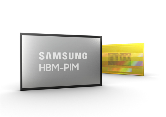
![HBM-PIM chip developed by Samsung Electronics for the first time in the world. Compared to the existing HBM2, the performance is doubled and energy consumption is reduced by more than 70%. [사진 삼성전자]](https://i0.wp.com/pds.joins.com/news/component/htmlphoto_mmdata/202102/17/fa6f073e-8a51-42e6-aa9e-54930231b275.jpg?w=560&ssl=1)
HBM-PIM chip developed by Samsung Electronics for the first time in the world. Compared to the existing HBM2, the performance is doubled and energy consumption is reduced by more than 70%. [사진 삼성전자]
Samsung Electronics has developed a next-generation memory chip that combines a memory semiconductor and an artificial intelligence (AI) engine. It is a semiconductor that adds a processor function necessary for operation in the memory.
Next-generation technology equipped with AI engine in memory
Double performance compared to the previous one, energy 70% ↓
“Expanding the PIM ecosystem in cooperation with customers”
Samsung Electronics announced on the 17th that it has developed the world’s first’HBM-PIM’ product that combines a memory semiconductor with a storage function and an AI processor into one. PIM (Processing-in-Memory) is a convergence technology that adds processor functions necessary for computational tasks inside the memory. Memory semiconductors function as information storage, and they are’hybrid semiconductors’ in which arithmetic functions (non-memory semiconductors) are combined.
An official from Samsung Electronics explained, “If HBM-PIM technology is installed in the AI system, the performance can be about twice as high as that using the existing HBM2 Aquabolt, and the system energy can be reduced by more than 70%.” HBM2 Aquavolt is a high-bandwidth memory semiconductor mass-produced by Samsung Electronics in 2018. It supports the existing HBM interface so that HBM-PIM can be used without changing hardware or software.
“HBM-PIM is a remarkable achievement in terms of performance and energy efficiency for AI applications,” said Rick Stevens, head of CELS research center at Argon National Laboratory.
HBM-PIM has improved performance by installing an AI engine in each bank (the smallest logical unit constituting the bank and main memory) inside the memory and maximizing parallel processing. Recently, as the application field of AI has expanded, the demand for high-performance memory has increased significantly, but it was difficult to overcome the limitations of the’phone Neumann structure’ with the existing memory. In the von Neumann architecture, the central processing unit (CPU) loads and executes instructions from memory, and then sequentially processes the storage again. The more data there is, the slower the speed. Samsung Electronics overcame this problem by maximizing parallel processing.
“HBM-PIM is the industry’s first AI-customized PIM solution that can maximize the performance of AI accelerators,” said Park Kwang-il, head of product planning team at Samsung Electronics’ memory division. said.
Samsung Electronics plans to perform performance verification by installing HBM-PIM in its customers’ AI accelerators by June this year. This content was published as a thesis at the International Society for Solid State Circuits (ISSCC), a world-class conference in the semiconductor field.
Reporter Choi Hyun-ju [email protected]
