Published in Science Journal, the results of joint research by researchers at the Institute of Basic Science, Hanyang University
Samsung Electronics sponsors research through Samsung Future Technology Promotion Project

(Seoul = Yonhap News) Samsung Electronics announced on the 29th that a research team supported by the Samsung Future Technology Promotion Project has succeeded in directly observing the nuclear generation process at the atomic level.
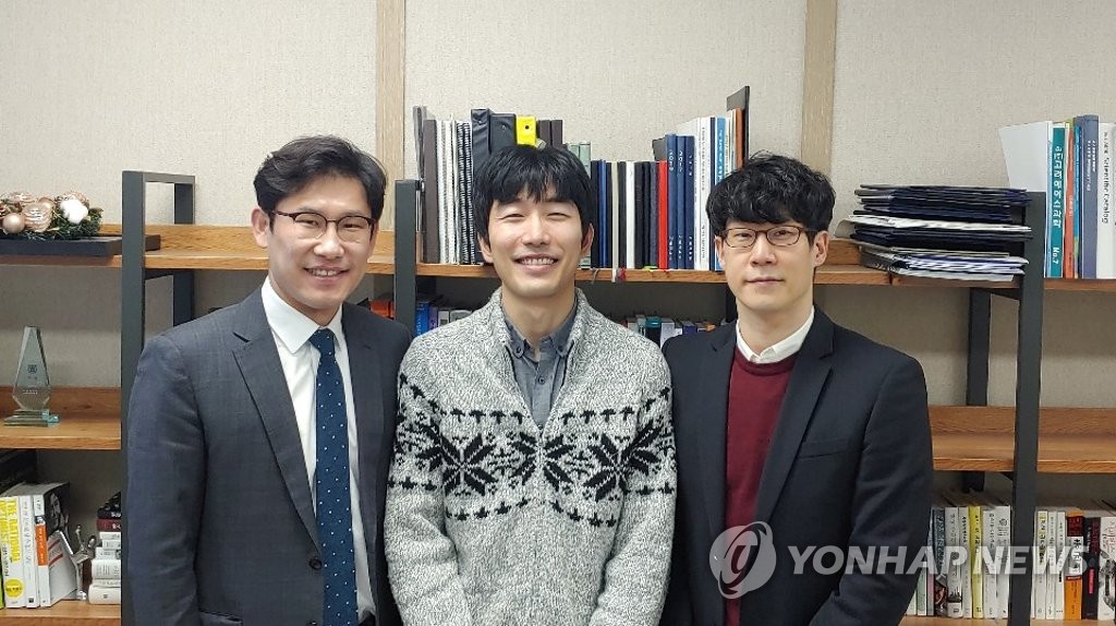
The photo shows Professor Jeong-Won Park of Seoul National University who led the study (from left), Dr. Seong-Ho Jeon, Erica Campus, Hanyang University, and Wonchul Lee, Erica Campus, Hanyang University. 2021.1.29
[삼성전자 제공. 재판매 및 DB 금지] [email protected]
(Daejeon·Seoul = Yonhap News) Reporter Park Joo-young and Kim Young-shin = Korean researchers succeeded in observing the process of nuclear formation for the first time in the world.
Research Fellow Park Jeong-won (Professor of the Department of Chemical and Biological Engineering, Seoul National University), a research fellow at the Nanoparticle Research Center at the Institute of Basic Sciences (IBS), announced on the 29th that it was the first to observe the process of’nucleation’ in which atoms gather to form crystals.
The research results, jointly conducted by the research team of the Research Institute of Basic Science, Professor Woncheol Lee’s team at the Erica Campus of Hanyang University, and the Lawrence Berkeley National Laboratory (LBNL) in the United States, were published on the day of the prestigious international journal’Science’.
This paper entitled’Reversible disorder-order transitions in atomic crystal nucleation’ was acknowledged for presenting the principle of nucleation, which has been a long-standing challenge in the academic world. .
Nucleation is the starting point of atoms gathering to form matter, but the size of the atoms is as small as a few angstroms (Å·10 billionths of a meter), and it is difficult to observe because it moves rapidly in milliseconds (ms·1 thousandths of a second).

(Seoul = Yonhap News) Research Fellow Park Jeong-won (Professor of Chemical and Biological Engineering, Seoul National University), Research Fellow Park Jeong-won (Professor of Chemical and Biological Engineering, Korea Institute of Basic Science) and Hanyang University’s Erica Campus, Professor Won-cheol Lee’s team, announced on the 29th that they succeeded in observing the nucleation process directly at the atomic level. .
The photo shows the process of growing gold atoms into crystal nuclei by repeating the amorphous and crystalline states observed using a high-speed transmission electron microscope. 2021.1.29
[기초과학연구원 제공. 재판매 및 DB 금지] [email protected]
The joint research team synthesized a nanomaterial that emits gold atoms when it receives an electron beam on thin graphene (a two-dimensional material separated from a layer of graphite), one atom thick.
Subsequently, the process of gold crystal formation was observed in real time using the world’s highest performance transmission electron microscope (TEM) possessed by LBNL.
The gold atoms that are emitted after receiving the electron beam from the transmission electron microscope are aggregated on a graphic thin film to form nanocrystals.
As a result of observation, it was found that the atoms form crystal nuclei by reversibly repeating the disorderly amorphous structure and the regularly arranged crystal structure.
Initially, the crystal nuclei, which were mostly in an amorphous state, grow and finally form a crystalline state.
This overturns the existing theory that crystal nuclei grow into a regular crystal phase from the beginning.
Research Fellow Park Jeong-won said, “We discovered a new principle of the nucleation process and tested it experimentally. In the initial stage when several atoms are clustered, the energy required to move back and forth between the crystalline phase and the amorphous phase is small, so the two states are repeated.” Explained.
Prof. Won-cheol Lee said, “We have succeeded in experimentally reproducing the very initial state of the thin film deposition process,” he said.

(Seoul = Yonhap News) Research Fellow Park Jeong-won (Professor of Chemical and Biological Engineering, Department of Chemical and Biological Engineering, Seoul National University), Research Fellow of the Nanoparticle Research Center, Korea Research Institute of Basic Science, and the research team of Professor Won-cheol Lee of Erica Campus of Hanyang University succeeded in observing the nucleation process directly at the atomic level for the first time in the world. Revealed.
The picture is a schematic comparing the existing nucleation process with the nucleation process observed in this study. 2021.1.29
[기초과학연구원 제공. 재판매 및 DB 금지] [email protected]
Samsung Electronics contributed to this research through the Samsung Future Technology Promotion Project.
Professor Park Jeong-won participated in this research with the support of the Samsung Future Technology Promotion Project and the Research Center Project of the Institute of Basic Science.
Prof. Park previously conducted research on’nano particle 3D proof photography technology development’ with the help of the Samsung Future Technology Promotion Project and the Institute of Basic Science, and the results were published in Science in April of last year.
The Samsung Future Technology Promotion Program has contributed 1.5 trillion won for 10 years since 2013, three times a year in research fields such as basic science, material technology, and information and communication technology (ICT) (free competition in the first and second half of the year, designated theme once a year). It is a public service project that selects and supports projects.
In line with the philosophy of fostering and supporting the science and technology field that will take responsibility for the future of Korea, Samsung has provided KRW 825 million in research funding for 634 projects from 2013 to the present through this project.
[email protected], [email protected]
Unauthorized reproduction-redistribution prohibited>
2021/01/29 07:44 sent
