IBS-Hanyang University joint research achievements published in the renowned academic journal’Science’
Samsung Electronics supports future technology development projects
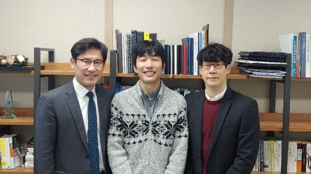
![Seoul National University Professor Park Jeong-won (from left), Hanyang University Erica Campus Dr. Seongho Jeon, Hanyang University Erica Campus Lee Woncheol. 2021.1.29
[사진=삼성전자 제공]](https://i0.wp.com/img.hankyung.com/photo/202101/01.25185687.1.jpg?w=560&ssl=1)
Seoul National University Professor Park Jeong-won (from left), Hanyang University Erica Campus Dr. Seongho Jeon, Hanyang University Erica Campus Lee Woncheol. 2021.1.29
[사진=삼성전자 제공]
Korean researchers succeeded in observing the world’s first nuclear process.
Research Fellow Park Jeong-won (Professor of the Department of Chemical and Biological Engineering, Seoul National University), a research fellow at the Nanoparticle Research Center at the Institute of Basic Sciences (IBS), announced on the 29th that it was the first to observe the process of’nucleation’ in which atoms gather to form crystals.
The research results, jointly conducted by the research team of the Research Institute of Basic Science, Professor Woncheol Lee’s team at the Erica Campus of Hanyang University, and the Lawrence Berkeley National Research Institute (LBNL) in the United States, were published on the same day of the world famous journal’Science’.
This paper, entitled’Reversible disorder-order transitions in atomic crystal nucleation’, was recognized for suggesting the principle of nucleation, which has been a long-standing challenge in the academic world.
The size of an atom is as small as a few angstroms (Å·10 billionths of a meter), and it moves rapidly in milliseconds (ms·1000ths of a second), making it difficult to directly observe the nucleation process with conventional technologies. Several theories explaining the mechanism of nucleation emerged, but there were limitations in proving through experiments.
![The picture is a schematic showing the process of forming gold nanocrystals after a substance emitting gold atoms forms crystal nuclei. 2021.1.29 [사진=삼성전자 제공]](https://i0.wp.com/img.hankyung.com/photo/202101/01.25185686.1.jpg?w=560&ssl=1)
The picture is a schematic showing the process of forming gold nanocrystals after a substance emitting gold atoms forms crystal nuclei. 2021.1.29 [사진=삼성전자 제공]
The collaborators designed an experiment to observe the nucleation process in real time at the atomic level. First, we synthesized a nanomaterial that emits gold atoms when an electron beam is received on a thin graphene film with a thickness of one atom.
Afterwards, the synthesized specimen was observed with the world’s highest performing transmission electron microscope (TEM) owned by the Lawrence Berkeley National Laboratory in the United States, and the process of gold crystal formation was observed in real time.
The gold atoms emitted after receiving the electron beam from the transmission electron microscope aggregate on the graphic film to form nanocrystals. As a result of observation, it was confirmed that the atoms reversibly repeat the two states: a randomly clustered lump structure (amorphous phase) and a regularly arranged crystal structure (crystalline phase) until a stable nucleus is formed.
Subsequently, as the size of the crystal nuclei grew, the reversible reaction became irreversible. This is contrary to the traditional nucleation theory that crystal nuclei grow in a regularly ordered crystal phase from the beginning.
In addition, the researchers also confirmed that as the size of the crystal nuclei grows, the probability of staying in the crystalline state increases. When the diameter was about 1 nm, it had a crystalline phase with a probability of 10%, but when the diameter exceeded about 2 nm, it existed as a crystalline phase with a probability of 90% or more. In other words, crystal nuclei, which were mostly amorphous at first, grow and finally form a crystalline state.
In addition, the researchers also confirmed that the longer the crystal nucleus stays in the crystal phase, the larger the nanocrystals are formed. For example, when a nanocrystal with an area of 2 nm² was formed, it was in the form of a crystal phase for only half the time, but when a nanocrystal with an area of 4 nm² was formed, the nuclei existed in the form of a crystal phase most of the time.
![Schematic comparing the existing nucleation process with the nucleation process observed in this study. 2021.1.29 [사진=삼성전자 제공]](https://i0.wp.com/img.hankyung.com/photo/202101/01.25185685.1.jpg?w=560&ssl=1)
Schematic comparing the existing nucleation process with the nucleation process observed in this study. 2021.1.29 [사진=삼성전자 제공]
Research Fellow Park Jeong-won said, “We discovered a new principle of the nucleation process and tested it experimentally. In the initial stage when several atoms are clustered, the energy required to move back and forth between the crystalline phase and the amorphous phase is small, so the two states are repeated.” Explained.
Prof. Won-cheol Lee said, “We have succeeded in experimentally reproducing the very initial state of the thin film deposition process,” he said.
In this study, Samsung Electronics(82,000 -2.03%)Has contributed through the Samsung Future Technology Promotion Project. The Samsung Future Technology Promotion Project has contributed 1.5 trillion won for 10 years since 2013, three times a year in research fields such as basic science, material technology, and information and communication technology (ICT) (free contest in the first and second half of the year, designated theme once a year). It is a public service project that selects and supports projects.
Reporter Kang Kyung-joo [email protected]
