UNIST, independently developed 4D complex nano microscope… Contributing to the development of next-generation electronic devices

The Ulsan Institute of Science and Technology (UNIST) announced on the 22nd that it has succeeded in controlling and observing 2D semiconductor nano wrinkles using a nanomicroscope independently developed by Professor Park Gyeong-deok’s research team in the Department of Physics.
With this technology, it is expected to contribute to the development of next-generation electronic devices such as paper-thin and bendable displays as it has been experimentally proven that nano wrinkles, which were considered defects of 2D semiconductors, have advantageous properties in manufacturing light emitting devices.
According to the research team, two-dimensional semiconductor materials are as thin as atomic, so wrinkles of several tens of nanometers (nm·1 billionth of a meter) are inevitable during the manufacturing process. The hatch is counted as an element.
Due to the small size of wrinkles, it is impossible to accurately analyze characteristics with conventional spectroscopic technology, and because there is no technology that can partially control characteristics precisely, commercialization of 2D semiconductors is slow.
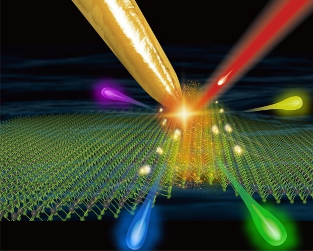
The research team solved this problem by independently developing the’active probe-enhanced photoluminescence nano microscope’ technology.
This nano-microscope can split the structural and optical properties of nano wrinkles into 15 nm level for precise analysis, and can freely control the properties.
Nano microscopy works by observing wrinkles finely with a gold probe.
The probe not only amplifies the weak luminous signal from the nano wrinkles, but also can precisely change the shape of the wrinkles. When the shape of the wrinkles is changed, various physical properties associated with it change.
With this technology, the research team identified the phenomenon of a’exciton funnel’ in which excitons, called’light particles’, gather into nano wrinkles of tungsten iselenide.
The research team explained that it was experimentally proved that the luminescence properties of nano wrinkles in which light particles are gathered into wrinkles are better than those without wrinkles.

Professor Park Gyeong-deok said, “This study analyzes the structural and optical properties of materials with ultra-high resolution in a three-dimensional space, and at the same time, combines atomic force microscopy technology to control the mechanical properties and electrical and optical properties of materials in real time. “We have developed a new paradigm for nano microscopes,” he said.
The research results were published online on the 11th in’Advanced Materials’, an international journal, and are scheduled to be officially published after being selected as a cover paper.
The original technology for nano microscopy has been patented.
/yunhap news
