Korea Electric Research Institute research team completes development of silicon carbide defect inspection technology

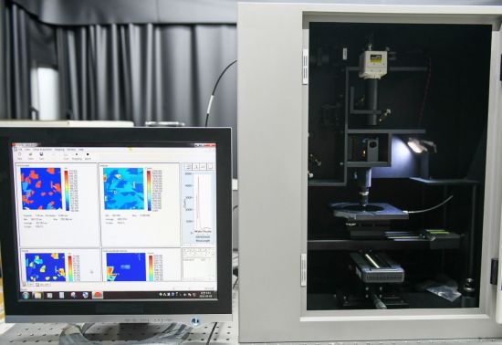
SiC material defect analysis equipment for power semiconductors. Photo courtesy = Korea Electric Research Institute (KERI).
[아시아경제 김봉수 기자]It is now possible to localize Japanese-made power semiconductor inspection equipment that dominated 80% of the global market. In the material, parts, and equipment war against Japan, there is one more foothold to counterattack.
The Korea Institute of Electrical Engineers (KERI) announced on the 8th that the Ph.
Power semiconductors are important parts of the industry that are essentially used wherever power is needed, and they play the same role as a muscle in terms of humans, such as controlling the direction of current and controlling power conversion. It is a high-tech material that forms the basis of eco-friendly industries such as electric vehicles and new and renewable energy, and is regarded as a key technology leading the digital-based fourth industry such as 5G mobile communication networks. In particular, it is used as an essential component for a high-performance inverter that connects a battery and an electric motor in an electric vehicle, and has recently attracted much attention.
Materials that maintain control efficiency, the core of power semiconductors, are being replaced by silicon carbide (SiC) from existing silicon (Si). SiC, which has excellent thermal and electrical characteristics, boasts excellent durability, versatility, operating temperature and speed, and high efficiency, and is rapidly replacing the existing silicon power semiconductor market.
However, SiC materials are regarded as one of the main causes of deteriorating the performance of semiconductor devices due to the invisible internal crystal defects (dislocations) due to the material properties. These crystal defects are so complex and difficult to identify, and sometimes the characteristics of the semiconductor device deteriorate from the beginning of driving, and in more serious situations, the characteristics gradually change during use, causing problems. For example, if a problem occurs in the power system site that is sensitive to accidents or the SiC power semiconductor of an electric vehicle running on the road, it can lead to serious human and property damage.
Therefore, it is important to develop a SiC power semiconductor with excellent performance, but an analysis technique capable of inspecting defects and solving various problems so as not to cause problems in the future is essential. The defects of the SiC material are not visible and the material is very hard, making it very difficult to observe. Currently, SiC material inspection equipment has high technical difficulty and entry barriers so that Japan occupies more than 80% of the global market. Since the equipment cost is also high, in Korea, it is only at the level of testing the performance with some wafer samples.
The research team developed the first technology in Korea to detect defects in SiC materials using the photoluminescece phenomenon. The PL analysis method analyzes the phenomenon in which excited electrons emit light of a specific wavelength when they return to their place. In other words, after transmitting ultraviolet (UV) energy to the SiC material, it is determined whether it is normal or not (crystal defects) by analyzing a specific wavelength emitted by electrons.
Originally, SiC is an indirect bandgap semiconductor material with low PL emission efficiency, and it was difficult to detect signals with equipment. However, the research team was able to develop a’SiC material defect analysis equipment for power semiconductors’ after efforts such as reducing PL loss through collaboration with Etamax, a company specializing in optical inspection equipment.
Unlike Japanese products that detect surface and internal defects by selecting two different wavelengths of light according to the inspection target and evaluation item, the KERI developed equipment can inspect various internal defects without destroying SiC materials with only one laser wavelength. have. Equipment performance, such as inspection precision (defect detection ability), showed a level of equal or higher level. The research team expects to be able to supply the inspection equipment price at half the price of Japanese products (about 1.4 billion won) through technology transfer and commercialization line construction with companies. The research team has completed the original patent application related to the developed technology.
Dr. Moon-Kyung Na said, “If we have focused on material source research and device development using this for preoccupying the highly difficult SiC power semiconductor market, now we have developed a variety of evaluation methods to ensure the reliability and quality of the developed products. Thus, we have built an integrated manufacturing line that leads to the’design-process-evaluation’ of SiC power semiconductors.” I will try to make it happen,” he said.
Meanwhile, according to the European market research institute IHS Market, the SiC power semiconductor market is expected to show an annual average growth of 32% from about $700 million last year to about $10 billion (about 11 trillion KRW) in 2030. do.
Reporter Kim Bong-soo [email protected]
