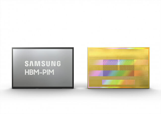
Samsung Electronics announced on the 17th that it has succeeded in developing the world’s first’HBM-PIM’ that combines a memory semiconductor and an artificial intelligence processor into one. It also reported that the related paper was published at the International Semiconductor Circuit Conference (ISSCC), the world’s most prestigious academic society in the field of semiconductors.
In the first half of the year, Samsung Electronics plans to complete the test verification by installing HBM-PIM in the artificial intelligence (AI) accelerators of customers. In addition, it plans to strengthen cooperation with customers to standardize the PIM platform and establish an ecosystem.
Processing in Memory (PIM) refers to a new concept fusion semiconductor that adds a processor function that takes charge of computing tasks inside the memory. Samsung Electronics succeeded in developing HBM-PIM with AI engine mounted on its second generation high-bandwidth memory (HBM2)’Aquabolt’ using PIM technology.
According to Samsung Electronics, when HBM-PIM is installed in an AI system, the performance of the system using the existing HBM2 can be more than doubled and the system energy can be reduced by more than 70%. As it supports the existing HBM interface, it is also an advantage that HBM users can build an AI accelerator system with HBM-PIM without changing hardware or software.
In recent years, the application area of AI is expanding in the computing market. In addition, as technology advances, the demand for high-performance memory continues to increase.
However, the existing memory had a limitation in that it was difficult to overcome the limitations of the von Neumann structure. Samsung Electronics’ HBM-PIM can perform computational processing inside the memory, reducing data movement between the central processing unit (CPU) and memory, increasing the energy efficiency of the AI accelerator system.
Related Articles

Evolving image sensor, getting smarter with AI technology

SK Hynix “Developing new memories such as ULM·AIM”

Investment of 125.3 billion won in AI semiconductors… “Cultivating it as the second DRAM”

Government launches special system semiconductor support program
In particular, Samsung Electronics installed an AI engine in each bank (the smallest logical unit when composing the main memory) inside the memory to maximize parallel processing to further increase the performance. Furthermore, HBM-PIM was commercialized by incorporating this into the DRAM process.
“HBM-PIM is the industry’s first artificial intelligence customized PIM solution that can maximize the performance of AI accelerators,” said Park Kwang-il, head of product planning at Samsung Electronics’ memory division. Will continue to build.”
☞ Terminology: von Neumann architecture
The von Neumann structure refers to a computer structure in which the CPU fetches and executes instructions from the memory, and stores the results back in the memory device. When the amount of data exchanged between the CPU and memory increases, there is a phenomenon that the work processing is delayed.
