Enter 2021.01.27 16:14 | Revision 2021.01.27 16:55
176 layers of high-laminated NAND also’surprise mass production’
World’s No. 1 and No. 2 Samsung and Hynix
Samsung and SK Hynix are scheduled for mass production in the second half

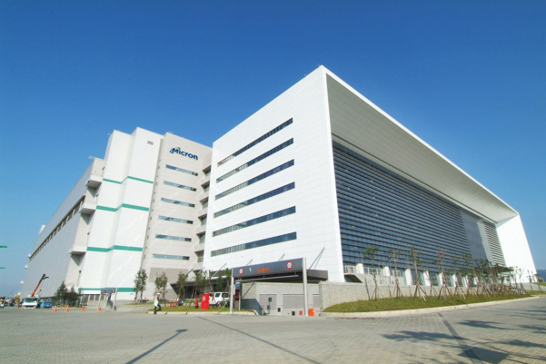
According to Micron on the 26th (local time), 1a DRAM is produced at a Taiwanese fab (factory). Vice President Scott Debore Micron said, “Compared to the existing 10-nano class 3G (1z) products, the density is improved by 40% and power efficiency is improved by 15%.
Micron is the first in the world to mass-produce and ship 1a DRAM. 1a DRAM refers to the 4th generation DRAM produced by the 10-nano process. Usually, DRAM makers named 1y, 1z, 1a, etc. whenever they reduce the circuit line width after shipping the 1st generation 1x. The next 5th generation will be 1b. It is estimated that Micron’s 1a DRAM is made in a 13-14nm process.

Earlier in November last year, Micron announced that it had shipped the world’s first 176-layer NAND flash. In December of last year, SK Hynix announced the completion of the 176-layer NAND flash development, but it has not reached mass production. Samsung Electronics currently does not apply more than 128 layers to NAND flash.
NAND Flash is evaluated as a technology that stacks high cells, which are spaces for storing data, and the number of cells is indicated according to the number of cell layers.

